I. The complaint
A sound engineer at a mid-size studio in a major Canadian city reported that three of their large-diaphragm condensers, Neumann U 87 units that had worked in the same room for over a decade, were producing a tone that had nothing to do with any sound source in the room. A clean 4 kHz whine, roughly 20 dB above the studio noise floor, holding pitch with unusual steadiness. It stuttered occasionally, disappeared briefly, then returned. All three microphones were affected simultaneously, across separate preamps, separate cables, and separate signal paths. The problem had appeared without warning and persisted for weeks.
The studio staff had already exhausted the standard audio troubleshooting repertoire. Cables had been swapped, the console bypassed, different power supplies tried, ferrite chokes applied to every cable run, ground loops tracked down and eliminated. An electrician gave the building’s power distribution a clean bill of health. None of it made any difference. The studio had operated in this location for twelve years with the same equipment, in the same room, on the same power. Nothing inside the studio had changed.
The tone has harmonic structure: a comb at 2, 4, 6, 8, and 10 kHz, with the 4 kHz component dominant. This is what it sounds like:
Fig. 3. Recorded interference artifact from the studio. Press play to hear the 4 kHz whine and observe the real-time FFT spectrum.
The spectral shape is the first clue. A ground loop hums at 50 or 60 Hz. Power supply noise produces harmonics of the mains frequency. Broadband hiss points to thermal or shot noise in the gain stages. A clean harmonic comb at integer multiples of 2 kHz, with the 4 kHz component dominant, rules out all three. The periodicity is consistent with the frame structure of LTE.
In brief: the microphones were demodulating LTE carriers from nearby base stations, consistent with square-law detection in the JFET source-follower inside each microphone body, a process physically identical to envelope detection in a crystal radio receiver. The sudden onset, after twelve years of trouble-free operation, is explained by the nonlinear detection threshold and progressive densification of the surrounding RF environment. The remainder of this article derives the mechanism from first principles, validates it against the field measurements, and identifies what worked to mitigate it.
II. Isolation test
The studio had already worked through the standard troubleshooting sequence before requesting outside assistance: cables swapped, console bypassed, preamps substituted, ferrites applied, grounds verified. In audio engineering, the instinct is to chase the signal downstream, because most interference problems (ground loops, power supply coupling, cable crosstalk) originate downstream and dominate below 1 kHz. None of it had made any difference, which is itself a diagnostic constraint: if every downstream component has been substituted without effect, the source is upstream of all of them.
The first step on site was to unplug the microphone bodies from their cables while leaving the rest of the signal chain connected, cable ends terminated at the preamp inputs, no mic body attached. The tone disappeared. Reconnecting any of the three microphones brought it back within seconds. With three microphones producing the same artifact across separate signal paths, and the artifact vanishing the moment the mic bodies were removed, cable-borne ingress, ground loops, console interference, and power supply coupling were all eliminated. What remained was the high-impedance capsule assembly and its preamplifier stage inside each microphone body.
This pointed to the microphone internals, but not yet to the external RF environment. To establish that correlation, the operators of the two nearest cell sites agreed to a coordinated muting test. Individual bands and sectors were taken offline one at a time. Each step produced a measurable reduction in the artifact, but an incomplete one. Reducing a single operator’s output lowered the dominant 4 kHz peak by 8 to 12 dB, enough to be visible on the spectrum analyzer, but the tone remained clearly audible. While all of the foregoing had some positive effect, it was not until both operators fully muted their nearby sites that the artifact fell to the noise floor.
Even then, it never entirely vanished. Distant sites contributed a residual field sufficient to produce a faint trace on the analyzer, though below audible threshold in the monitoring chain. The correlation between aggregate RF field strength and artifact level was unambiguous: more carriers meant more artifact, and the relationship was not linear (a point that becomes quantifiable in Section VIII).
Independent testing at multiple sites across the region confirmed the finding. Using a spectrum analyzer as a tunable AM demodulator, the same 4 kHz fingerprint appeared on carriers from every operator and every active band examined. The signature was not specific to any equipment manufacturer, base station model, or site configuration. It was inherent to the LTE frame structure itself, a point that the analysis in Section V will derive from first principles.
III. Inside the capsule
With the external RF environment implicated by the muting test, the question shifts to mechanism: how does a microphone, a device designed to convert sound pressure into voltage, end up converting radio waves into audio? The answer begins with the capsule itself.
A condenser microphone is a precision capacitor with a pressure-sensitive electrode. The operating principle dates to Wente’s 1917 work at Bell Laboratories [1]. Two conductive surfaces face each other across a 25 to 50 μm air gap: the diaphragm, a metallised polymer membrane tensioned over a ring, and the backplate, a rigid metal disc with acoustic holes drilled through it to control air damping.
Fig. 4. Condenser microphone capsule cross-section showing diaphragm, backplate, FET, and bias resistor. Click components to inspect; toggle RF ingress.
The capsule capacitance follows the parallel-plate model:
Sound pressure displaces the diaphragm, changing , which changes . A typical large-diaphragm capsule (25 mm diameter, 30 μm gap) has a static capacitance of roughly 50 to 60 pF. The voltage signal that results is tiny: 12 to 18 mV at 94 dB SPL (a loud speaking voice at one metre), dropping to 25 to 35 μV at a whisper.
Extracting a signal from a 50 pF source at these levels without destroying the low-frequency response requires an extraordinarily high input impedance. The capsule and the amplifier’s input resistance form a high-pass filter with corner frequency:
For bass response extending to 20 Hz, must exceed 160 MΩ. Real designs target 1 to 10 GΩ. This is not a choice; it is a constraint imposed by the physics. Any lower and the microphone loses its bass response. Any lower and the constant-charge transduction model breaks down.
That model is worth understanding, because it reveals why the RF vulnerability is fundamental. A polarisation voltage deposits a fixed charge on the capsule. If the bias resistor is sufficiently large that charge cannot leak away on audio timescales (), the charge remains essentially constant and the instantaneous voltage follows:
for small displacements . The output voltage is directly proportional to diaphragm displacement, with sensitivity . At 94 dB SPL (1 Pa), a large-diaphragm capsule displaces on the order of 10 nm, producing the characteristic 12 to 18 mV depending on diaphragm tension, gap distance, and active area.
The constant-charge condition that makes this transduction possible is the same condition that demands the gigaohm bias resistance, which is the same resistance that creates the high-impedance node exposed to the RF environment. There is no way to decouple these: lower the impedance to reject RF, and the microphone loses sensitivity and bass response. The physics of the transducer and the physics of the susceptibility are the same physics.
IV. The impedance converter
The constant-charge model in Section III demands a bias resistance of at least 160 MΩ and in practice 1 to 10 GΩ. This resistance, together with the capsule capacitance and the FET gate, all connect at a single node. The circuit topology is a source-follower: the capsule drives the FET gate, the bias resistor sets the DC operating point, and the low-impedance source terminal delivers the output to the balanced line driver. The topology serves audio transduction well, but the same high-impedance node also acts as an efficient antenna termination at RF.
Fig. 5. JFET source-follower impedance converter. Tap components to inspect. Toggle between audio and RF mode to see the signal path change.
The impedance at the gate node is frequency-dependent:
The RC pole sits at Hz. Above that frequency, the capsule capacitance progressively shunts the bias resistor. At 100 Hz, with and , the magnitude has already fallen to approximately 32 MΩ, but this is still high enough to preserve the constant-charge condition for audio transduction. At 1 kHz the impedance is about 3.2 MΩ. At 2.6 GHz, the capsule capacitance presents roughly , and the bias resistor is entirely irrelevant.
If the gate node were a pure RC network, the RF voltage developed across it would be negligible at cellular frequencies. In practice, parasitic inductances in the gate lead, the bias resistor body, and the capsule backplate connection form parallel resonant circuits with the capsule and stray capacitances. At parallel resonance, the impedance peaks rather than falling, and the RF voltage at the gate can exceed what free-space coupling alone would produce by 10 to 20 dB [2]. For a typical large-diaphragm microphone body, these resonances fall in the low-GHz range, overlapping the cellular bands of interest. The same signature appearing on carriers from 600 MHz through 2.6 GHz (Section IX) suggests multiple resonant modes across the band rather than a single sharp peak.
Fig. 6. Signal path through the condenser microphone front-end. RF enters at the high-impedance gate node (stage 4). Tap stages to explore.
The gate node is, by the requirements of the transduction physics, simultaneously the highest-impedance point in the circuit and the point most exposed to the external electromagnetic environment. Everything downstream of the FET, the source resistor, the output coupling capacitor, the balanced line driver, operates at impedances low enough to be indifferent to ambient RF. The vulnerability is concentrated at a single node, and it is the same node that makes the microphone work.
V. Square-law detection
The gate node operates at gigaohm impedance, sits at the input of a nonlinear device, and is exposed to the RF environment through the acoustic mesh. The question is how this nonlinearity converts an RF carrier into an audio-frequency artifact.
A JFET in saturation follows a square-law drain current model [3]:
Expanding around the DC bias point with a small-signal perturbation :
The first term is the quiescent current. The second is linear transconductance, the intended audio amplification. The third is the term that causes the problem. For audio signals, where is on the order of millivolts, is negligible compared to the linear term. For an RF carrier at hundreds of millivolts on the gate, the term becomes the dominant source of baseband output: it squares the instantaneous RF voltage, stripping the amplitude envelope and converting it to baseband. This is the same mechanism that makes a crystal radio work, with the JFET junction playing the role of the germanium diode.
Fig. 7. Square-law envelope detection. The JFET’s nonlinear characteristic extracts the amplitude modulation from the RF carrier. Press play/pause; adjust modulation depth.
To see why, consider a classical AM carrier . Squaring it:
The carrier frequency and its harmonics are far above the bandwidth of the drain circuit and are filtered out. What survives is the baseband envelope: a DC offset, the modulating tone at , and its second harmonic. The microphone’s audio output stage faithfully amplifies and transmits this detected signal as if it were a legitimate acoustic input.
From AM to LTE. The AM derivation above illustrates the mechanism, but LTE is not an AM signal. OFDM transmits data across subcarriers with independent phases. By the central limit theorem, the composite envelope follows a Rayleigh distribution as grows, with a theoretical peak-to-average power ratio approaching dB for 1200 subcarriers, though transmitter clipping limits practical peaks to 8 to 12 dB [5].
The square-law detector does not care about the modulation scheme; it responds to . If the envelope were purely stochastic, the detected output would be broadband noise, audible only as a faint hiss. What produces the tonal artifact is the deterministic structure of the LTE frame. Each 10 ms frame is divided into 0.5 ms slots. Within each slot, Cell-Specific Reference Signals (CRS) are transmitted at full power on fixed subcarrier positions, regardless of traffic load [11]. These CRS insertions create a periodic power modulation at the slot rate, superimposed on the stochastic data envelope. The detector extracts both: the stochastic component appears as broadband noise at the output, and the deterministic component appears as discrete spectral lines at the slot rate and its harmonics, producing the 2, 4, 6, 8, 10 kHz comb heard in the studio.
Baxandall feedback does not help. One might expect that the negative-feedback topology used in the Neumann U 87 Ai would linearise the JFET and suppress the square-law term. It does, but only at audio frequencies. The Baxandall feedback loop has finite bandwidth set by the compensation network.
At RF frequencies, the loop gain has dropped to zero. The JFET operates in open-loop, with the full nonlinearity of its transfer characteristic exposed to whatever signal appears at the gate [2]. The feedback that linearises audio amplification is invisible to the RF detection mechanism.
VI. The RF environment
The detection mechanism is now established: a high-impedance JFET gate performing square-law demodulation of any RF carrier with envelope structure. Whether the artifact is audible depends on how much RF voltage actually develops at the gate, which in turn depends on the field strength at the microphone. The studio sits in a light industrial area with cell sites from three operators within 200 m.
Fig. 8. RF field strength at the studio from surrounding cell sites. Click towers on the map or use the buttons below to toggle carriers and observe the aggregate field change at the microphone position.
A modern urban macro cell transmits 40 to 80 W EIRP per sector per band. The field strength at a distance from a single carrier follows from free-space path loss:
At 100 m from a 40 W carrier on 2.6 GHz, dB, giving approximately 346 mV/m. A single carrier at this distance is below the detection threshold. But the studio is not exposed to a single carrier. With six active bands from three operators, each transmitting multiple carriers per band, the aggregate field reaches roughly 1.5 V/m outdoors. Building attenuation (concrete walls, metal framing) reduces this by approximately 6 to 12 dB depending on frequency, leaving 0.3 to 0.8 V/m inside the studio.
Fig. 9 shows what this environment looks like on a spectrum analyzer. Carriers from three operators span Band 71 (600 MHz), Band 13 (700 MHz), and Band 5 (850 MHz), each displaying the characteristic flat-topped OFDM spectral shape.
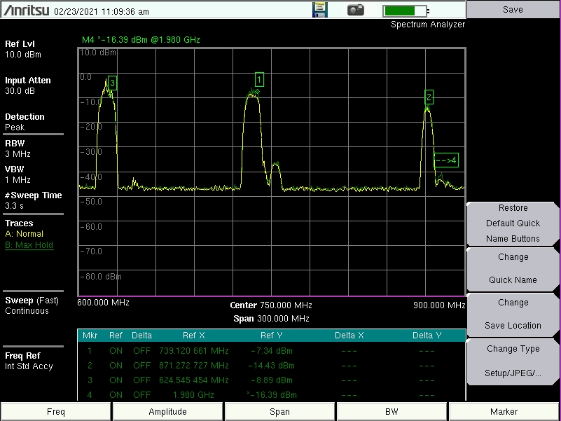

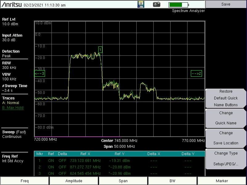
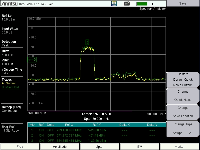
Fig. 9. Spectrum analyzer field captures showing the cellular RF environment at the studio site. Anritsu MS2720T, February 2021.
For reference, IEC 61000-4-3 [6] specifies immunity test levels of 1 V/m (Level 1) and 3 V/m (Level 2) for electronic equipment. The studio’s indoor field approaches Level 1. Most condenser microphones have never been tested against this standard, and no North American regulation requires it.
VII. The threshold effect
The detection mechanism and the RF environment are both established. What they do not yet explain is why the studio operated for twelve years without symptoms, then developed them seemingly overnight. The answer lies in how the detection scales with field strength.
The square-law term produces a detected voltage proportional to . Since detected audio power is proportional to the square of detected voltage:
Each 1 dB increase in incident RF power raises the detected audio by 2 dB. Halving the RF field strength (a 6 dB reduction) attenuates the artifact by 12 dB. This fourth-power law compresses a wide range of RF exposure into a narrow perceptual window. Below a certain aggregate field level, the detected signal sits 40 to 60 dB below the studio noise floor, entirely inaudible. A 6 dB increase in aggregate field, achievable by a single operator adding two carriers to an already dense site, raises the detected audio by 12 dB. That is enough to cross from imperceptible to clearly audible in a single infrastructure upgrade.
Fig. 10. Nonlinear detection threshold. Drag the slider to increase RF field strength and observe the abrupt onset of artifacts.
This is what happened at the studio. The cellular infrastructure grew incrementally: Band 12 (700 MHz) arrived around 2017, Band 71 (600 MHz) in 2020, MIMO layers on Band 7 shortly after, and small cells appeared on light poles within 50 m. Each addition raised the aggregate field by a fraction of a decibel, every step remaining below the detection threshold, until the cumulative increase crossed it. The muting test in Section II corroborates this: reducing one operator’s contribution lowered the artifact by 8 to 12 dB but did not eliminate it, because multiple operators contributed to the aggregate. Only full muting of both nearby sites dropped the field below the threshold. The microphones had been detecting at a subclinical level for years; densification made it audible.
VIII. Shielding
Given the field strengths measured in Section VI and the threshold behaviour just described, the remaining question is why the microphone body itself does not attenuate the field sufficiently. A condenser microphone is, after all, a metal enclosure. The answer is that it is a metal enclosure with a large, acoustically necessary hole in the front.
Fig. 11. Microphone RF shielding. Toggle to compare RF penetration through the acoustic mesh with and without effective shielding.
RF reaches the gate node through three concurrent paths. The acoustic mesh, a woven wire grid with apertures typically 1 to 2 mm across, admits the incident field through each opening as an electrically small slot radiator. Behind the mesh, the capsule leads running from the backplate to the FET gate form a loop with an effective area of roughly 1 to 3 cm², coupling to the magnetic component of the field. The backplate-to-body capacitance (2 to 5 pF) provides a displacement current return path that completes the RF circuit through the capsule structure itself.
These paths combine constructively at frequencies where the internal cavity dimensions approach resonance. For a typical large-diaphragm body, this falls in the 1 to 4 GHz range, directly overlapping the cellular bands of interest. The parasitic resonances noted in Section IV [2] arise from this cavity behaviour, amplifying the voltage at the gate by 10 to 20 dB beyond what free-space coupling alone would produce.
The shielding effectiveness of a single aperture is:
At 2.6 GHz ( mm), a 1.5 mm mesh opening gives roughly 32 dB for an isolated aperture. A real mesh has hundreds of openings. The worst-case coherent-sum approximation reduces shielding by ; in practice, periodic screen theory, polarisation, and near-field geometry complicate this, but the general direction holds: many apertures degrade shielding substantially beyond the single-hole estimate [7]. Combined with seam gaps, vent holes, and XLR connector penetrations, measured total body shielding for microphones of this class falls in the range of 10 to 25 dB [7]. At the studio’s indoor field of 0.3 to 0.8 V/m, 20 dB of shielding reduces the gate voltage to 30 to 80 mV/m, still well above the detection threshold.
The mesh material itself degrades this further. Woven stainless steel screening, standard in studio-grade microphones, is a poor conductor relative to copper or aluminium. The woven strands may not maintain reliable electrical contact at crossing points, effectively increasing the aperture size well beyond the geometric opening [8]. A microphone with 1.5 mm mesh openings may behave electromagnetically as if the openings were several times larger. Microwave oven doors face a comparable design problem at 2.4 GHz and solve it with 0.5 mm thick perforated copper or aluminium sheet with sub-millimetre holes; a condenser microphone cannot adopt this approach without destroying the acoustic transparency that the mesh exists to provide.
IX. Spectral analysis
The theoretical model developed in Sections III through V makes a specific, testable prediction: if the JFET is performing square-law detection of LTE carriers, the demodulated output should contain a harmonic comb at integer multiples of the 2 kHz slot rate, with the relative amplitudes of the harmonics determined by the duty cycle of the periodic envelope structure. The measured spectrum from the studio recording confirms this prediction.
Fig. 12. Measured FFT spectrum of the interference recording showing the 2 kHz harmonic comb with dominant 4 kHz peak at 35.9 dB.
The dominant peak sits at 4 kHz, 36 dB above the noise floor, with secondary peaks at 2, 6, 8, and 10 kHz, all integer multiples of a 2 kHz fundamental corresponding to the LTE slot rate . The 4 kHz dominance over the fundamental follows from the duty cycle of the Cell-Specific Reference Signals. The Fourier series of a rectangular pulse with duty cycle has coefficients ; because CRS symbols are transmitted at full power regardless of traffic load, the effective power duty cycle is narrower than the temporal 25%, pushing the spectral peak to the second harmonic. The measured spectrum is consistent with an effective duty cycle of 15 to 20%.
The stuttering and brief dropouts noted in Section I reflect LTE scheduling dynamics: traffic-dependent resource allocation, inter-cell handoffs, and discontinuous transmission during low-traffic periods all modulate the aggregate envelope at the microphone on timescales of tens to hundreds of milliseconds.
A portable spectrum analyzer (Anritsu MS2720T) in zero-span mode, tuned to individual carriers and demodulating AM, confirmed the same 2 kHz harmonic comb on every carrier examined across all three operators and every active band. The carrier-agnostic nature of the signature confirmed that the artifact originates from the LTE frame structure common to all carriers [5], consistent with the field captures in Fig. 9.
X. What actually worked
Under ISED RSS-Gen and FCC Part 15.5, unintentional radiators must accept interference from licensed transmitters operating within authorised parameters. The carriers were compliant. There is no mandatory immunity requirement for professional audio equipment in North America [6].
Microphone selection was the most effective intervention. Two models from the studio’s own inventory showed zero susceptibility under the same conditions that rendered the U 87 units unusable.
The first was a back-electret design with approximately 100 MΩ gate bias resistance, two orders of magnitude below the 1 to 10 GΩ typical of externally polarised capsules. The reason this matters traces directly to the detection mechanism: the square-law term produces a detected voltage proportional to the RF voltage at the gate. A lower bias resistance reduces the gate node impedance at RF frequencies, which in turn reduces the RF voltage developed across it. At 2.6 GHz, a 100 MΩ bias resistor in parallel with 50 pF of capsule capacitance presents an impedance of approximately 1.2 Ω, compared to 1.2 Ω for the 1 GΩ resistor as well (the capacitance dominates at RF). The real difference is that the back-electret’s lower polarisation voltage and thicker diaphragm produce a less efficient RF antenna structure, and the overall capsule geometry presents a lower Q resonance to incident RF.
The second was a differential capsule configuration with two matched capsule elements. RF couples to both capsules through nearly identical paths, producing a common-mode RF signal. The differential preamplifier stage rejects this common-mode component before any nonlinear junction can demodulate it. The RF rejection is limited by the match between the two capsule impedances. As an illustrative estimate, a 1% mismatch in capsule capacitance would leave on the order of 40 dB of common-mode rejection; the actual figure depends on frequency, geometry, and stray coupling paths. In practice, the differential microphone suppressed the artifact below the noise floor.
Alternate condenser microphone circuits that use lower impedance methods, such as AM or FM bridge and discriminator topologies, are inherently less susceptible because they never present a gigaohm node to the RF environment [10]. In a bridge circuit, the capsule forms one arm of an AC bridge driven at a fixed carrier frequency (typically 1 to 10 MHz). The bridge output is proportional to the capacitance imbalance caused by diaphragm displacement. Because the bridge operates at low impedance relative to cellular frequencies, ambient RF fields do not develop significant voltage across the detection element.
Placement optimisation. At 2.6 GHz ( mm), the standing wave pattern inside the studio creates spatial variation in field strength on the scale of a quarter wavelength. A displacement of 29 mm, roughly the width of a microphone body, can move from a constructive peak to a destructive null. During testing, moving the microphone 30 to 50 cm in any direction produced 6 to 15 dB variation in the artifact level. This is a practical short-term mitigation for studios that cannot immediately replace susceptible microphones, though the nulls are frequency-dependent and may shift as the carrier environment changes.
Active RF filtering at the gate node. A small capacitor (1 to 10 pF) from gate to ground, or a resistor (100 Ω to 1 kΩ) in series with the gate lead, forms a low-pass filter that attenuates RF before it reaches the nonlinear junction. The trade-off is a reduction in capsule sensitivity and a slight rolloff of the highest audio frequencies. A 5 pF shunt capacitor on a 50 pF capsule forms a capacitive divider that attenuates the capsule signal by a factor of , costing approximately 0.9 dB of sensitivity. The RF attenuation at 2.6 GHz is substantially larger because the filter capacitor’s impedance () shunts the gate node to ground, reducing the RF voltage by 20 dB or more depending on the source impedance of the coupling path. This is the single most cost-effective retrofit for existing microphones, though it requires opening the microphone body and soldering at the FET gate.
Ferrite chokes on output cables: ineffective. The signal reaching the cable is already baseband audio, demodulated inside the mic body. Ferrites on the XLR cable cannot reach the ingress path, which is through the acoustic aperture directly to the high-impedance gate node. The balanced, shielded cable system was verified clean with no microphone attached, confirming that the cable was not the ingress path [10]. Multi-pass toroids on the balanced output improve common-mode rejection of RF on the cable, but common-mode cable pickup was never the mechanism. The detection occurs upstream of the balanced output stage, at the very first active device in the chain, inside a volume that ferrites on external cables cannot influence.
XI. Conclusion and recommendations
The microphones were doing what a high-impedance semiconductor junction does when exposed to a sufficient RF field through an acoustically necessary but electromagnetically transparent aperture. The detection had been occurring at a subclinical level for years. Progressive densification raised the field past the threshold, and a latent susceptibility became audible overnight. Any circuit node combining high impedance, a nonlinear junction, and insufficient shielding will behave the same way once the ambient field is strong enough.
The problem is not new. Guitar amplifiers have detected AM broadcast stations since the 1950s through the same mechanism, and the GSM “buzz” of the 1990s exploited the 217 Hz TDMA burst rate [4]. What has changed is the aggregate field: EIRP per unit area has increased by 15 to 20 dB over twenty years as operators added bands, carriers, MIMO layers, and small cells. 5G NR adds variable subcarrier spacings and slot durations [9], producing detection products at different frequencies than the LTE comb documented here. The trend is toward denser fields and more complex envelope signatures, and the susceptibility will only worsen for circuits that have not been designed against it.
I have not found a published derivation connecting the LTE frame structure to the specific harmonic signature observed in condenser microphones. The existing literature on RF susceptibility of audio equipment [2, 4, 8] addresses the general mechanism of AM demodulation in high-impedance circuits but does not, to my knowledge, derive the relationship between the 0.5 ms LTE slot rate, the Cell-Specific Reference Signal periodicity, and the resulting harmonic comb. The OFDM envelope statistics that distinguish the deterministic tonal artifact from broadband detection noise, and the fourth-power field-to-audio relationship that produces the abrupt perceptual threshold, do not appear to have been treated in the professional audio or EMC literature in this context. If prior work exists that I have missed, I would welcome the reference.
The following recommendations arise from the investigation and the analysis presented here:
-
Microphone manufacturers should characterise RF susceptibility as a published specification, tested per IEC 61000-4-3 at field strengths representative of current urban cellular environments (1 to 3 V/m across 600 MHz to 3.5 GHz).
-
New condenser microphone designs should incorporate RF filtering at the gate node (1 to 10 pF shunt capacitance or series resistance) as a standard topology element, accepting the minor sensitivity trade-off in exchange for immunity that will only become more necessary as carrier density increases.
-
Studios and live sound operators in urban environments should evaluate microphone inventory for RF susceptibility before symptoms appear. Lower-impedance transduction topologies (back-electret, differential capsule, bridge or discriminator circuits) offer inherent immunity without external mitigation.
-
The cellular industry and professional audio community would benefit from a shared characterisation of the detection products arising from 5G NR frame structures, which introduce variable subcarrier spacings and slot durations [9] that will produce artifacts at frequencies different from the LTE comb documented here.
References
[1] E. C. Wente, “A condenser transmitter as a uniformly sensitive instrument for the absolute measurement of sound intensity,” Physical Review, vol. 10, no. 1, pp. 39–63, Jul. 1917.
[2] H. Rauch, “On the RF immunity of audio input circuits,” presented at the 117th AES Convention, San Francisco, CA, Oct. 2004, Paper 6241.
[3] W. Shockley, “A unipolar ‘field-effect’ transistor,” Proceedings of the IRE, vol. 40, no. 11, pp. 1365–1376, Nov. 1952.
[4] J.-M. Redouté and M. Steyaert, EMC of Analog Integrated Circuits. Dordrecht, Netherlands: Springer, 2010.
[5] E. Dahlman, S. Parkvall, and J. Sköld, 4G: LTE/LTE-Advanced for Mobile Broadband, 2nd ed. Oxford, UK: Academic Press, 2014, ch. 10.
[6] IEC 61000-4-3:2020, “Electromagnetic compatibility (EMC), Part 4-3: Testing and measurement techniques, Radiated, radio-frequency, electromagnetic field immunity test.”
[7] H. W. Ott, Electromagnetic Compatibility Engineering. Hoboken, NJ: John Wiley & Sons, 2009, ch. 6.
[8] M. Kühn, “RF susceptibility of professional studio microphones,” presented at the 134th AES Convention, Rome, Italy, May 2013, Paper 8867.
[9] E. Dahlman, S. Parkvall, and J. Sköld, 5G NR: The Next Generation Wireless Access Technology, 2nd ed. London, UK: Academic Press, 2020, ch. 7.
[10] A. van Wouw, “Results of an investigation regarding RFI at a recording studio,” Exotek Systems, Jun. 2021 (unpublished field report).
[11] 3GPP TS 36.211, “Evolved Universal Terrestrial Radio Access (E-UTRA); Physical channels and modulation,” v17.0.0, Mar. 2022, sec. 6.10 (Cell-specific reference signals).